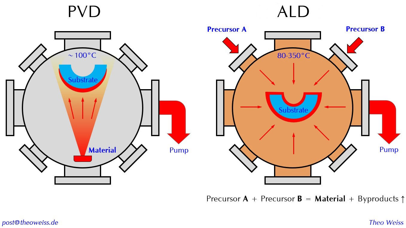
PVD vs ALD
Atomic Layer Deposition (ALD) is an advanced form of Chemical Vapor Deposition (CVD) vacuum coating technique that has established itself in the thin film deposition industry, especially in challenging metamaterial, MEMS, and semiconductor manufacturing. Nowadays ALD is a key technology that continues to push the boundaries of the empirical "Moore's law".
Recently, ALD has been successfully adapted for innovative photonic and laser-optical applications, where exceptional film uniformity and angstrom-level thickness control are required. As a surface-sensitive technique, ALD allows the coating of nearly any 3D-shaped object, including strongly curved shells or high aspect ratio trenches and wells. Typical examples of such challenging optical components include ball lenses, domes, rods, tubes, axicons, and complex multi-sided prisms.
In contrast, widely used physical vapor deposition (PVD) techniques, such as evaporation and sputtering, deliver coating material unidirectionally from a point source, leading to gradient thickness distribution, shadowing effects, and a lack of uniform all-around coating. ALD overcomes these limitations and has proven its reliability in achieving high precision and uniformity, particularly in semiconductor fields where the challenge is not only to achieve homogeneity over the outer shape but also within the microstructures at the nanometer scale.
PVD vs ALD
As previously mentioned, ALD is a chemical technique where surface reactions play a crucial role. In these reactions, two gaseous chemicals, known as precursors, react in a sequential, self-limiting manner only at the preheated surface (80-350°C), forming the desired solid film. The chemical nature of the growth process is responsible for the resulting near-stoichiometric, pinhole-free, dense films, enhancing surface smoothness, coating adhesion, and acting as a moisture barrier.
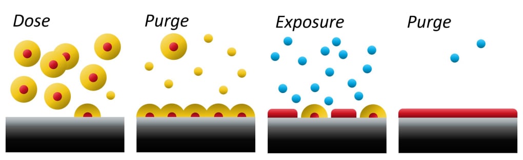
Atomic Layer Deposition - is a chemical process based on sequential, self-limiting surface reactions.
To achieve thicker films, the deposition sequence has to be repeated multiple times, monolayer-by-monolayer, using the same or different precursors. The self-limitation is an important feature of ALD that ensures high run-to-run repeatability of the deposition process.
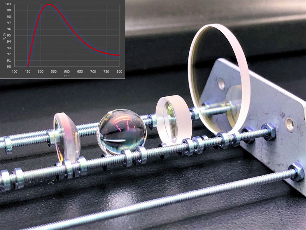
ALD coated Lenses with AR@532nm
With a wide range of standard materials available, such as Al2O3, ZnO, TiO2, HfO2, ZrO2, SiO2, Y2O3, and Ta2O5, ALD enables the coating of nearly any 3D surface at nano-, micro-, and macro-scales. It is effective even for high aspect ratio or strongly curved surfaces, allowing all surfaces to be coated in one run, with the option to protect some areas if needed.
Moreover, ALD facilitates the creation of new artificial materials, including thin and ultra-thin multilayer systems (nano-laminates) and films modified with sub-nanometer thin dopant layers.
Typical ALD Applications:
• Optical
• Functional
• Protective
• Decorative
Publication:
Th. Weiss et al., Atomic Layer Deposition for coating of complex 3D optics – from theory to praxis, Optik & Photonik, 12: 42–45, 2017